
c23. QRP experimental techniques II,
"transmitters"
List of related pages:
 a. Antenna
technik
a. Antenna
technik
b. Radio surplus equipment for
amateur radio operation
c. Amateur radio technik
c18. CW handpumps, paddles and
elbugs
c21 QRP page 1
c61. Components and store
d. VHF/UHF/SHF technik
L. VLF technik
m. Measuing instruments
m11. Grid-dip-meters and xtal testers
n18. Experiments
with ceramic resonators for IF filters
and variable oscillators (QRP pages)
n23. Building
lowcost xtal filters
Low cost solidstate power amplifiers
When considering the design of solidstate power amplifiers
with all their problems of accurately-matched loads,
susceptibility to transient overloads, parasititcs and other
forms of destructive self-oscillation, not to mention the high
cost of devices capable of high-power operation, most amateurs
tend to play safe and follow closely the techniques closely the
techniques currently favoured by professional designers. This is
understandable but is not necessarily the best policy for those
seeking ways out of using the older rf power devices that can now
be acquired for a fraction of the cost of
"state-of-the-art" devices. With some shopping around
it is possible to build a power amplifier of 10W rating at better
W/£ ratio than by using newly-bought valves and high-voltage psu
(though I stick to my formerly expressed beliefs that the valve
approach is still a good deal easier at and above this power
level).
Almost 20 years ago, TT, and subsequent editions of ART, drew
attention to what was then described as an "improved
transistor amplifier circuit" in the following terms:
Most transistor power amplifiers use the common-emitter
arrangement, corresponding most closely the the standard valve
(grounded cathode) circuit, on account of the high gain; others
use the common-base configuration on account of its higher
maximum frequency for a given transistor; or the common-collector
circuit wich allows direct metallic contact between the
transistor case and the heatsink or chassis.
"The distribution of the desirable characteristics among the
three standard circuits has encouraged some designers to try and
produce hybrid arrangements combining as many possible good
points into a single circuit".
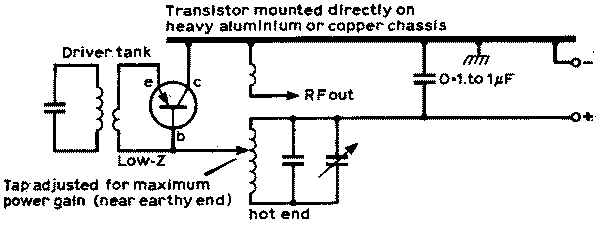
Fig.1. A hybrid form of solidstate power amplifier using grounded
collector. This was described for use with early pnp power
transistors in 1964.
One such approach is that described by Irving Gottlieb in
Electronic Industries August 1964: Fig.1. This circuit, is
claimed, has been developed using 2N1908 pnp device, and the
author states that he obtained about 10W output power power on
7MHz band using a transmitter consisting of a 2N697 co, 2N1907 ba
and 2N1908 pa. The efficiency and thermal electrical
characteristics of this circuit are claimed to be outstanding.
The author admits that some experimentation will usually be
needed to achieve best results but states that, once the input
and output impedances have been optimized, stability is almost
unaffected by driver or load variations, or by changes in the
supply voltages.
It was also claimed that such amplifier could be amplitude
modulated alomst 100% by means of a transformer winding inserted
in the positive dc lead, provided that the supply voltage was
suitably reduced. However, I have not heard of anybody using this
type of amplifier for many years. Indeed little attention has
been given to either this 'hybrid' configuration or the basic
common-collector arrangement during the pasta decade. G3VA,
Technical topics, Radcom January 83 pp41.
Grounded-collector 14MHz linear.
In view of the above notes, it was all the more interesting to
receive from LA8AK a description of a 14Mc/s solidstate linear
power amplifier using the 'grounded collector' configuration.
This amplifier was assembled in order to test what could be
achieved using low-cost BD139 transistors which a sometimes
available at low cost, an alternative is BD135. LA8AK recalls
that while the grounded-collector arrangement was occasionally
used by amateurs 15-20 years ago, it is seldom found mentioned.
To the best of his recollection, he has never seen it proposed
for linear operation. In practical terms the amplifier is not
very different from conventional grounded-emitter configuration,
but offers useful advantages.
The LA8AK test amplifier is shown in Fig.2, and incorporates a
number of ideas suggested originally by LA7MI Stein Torp, LA8AK
writes:
"Instead of an rfc in the supply lead, it uses a low-Q
resonant circuit to provide greater stability; LA7MI burnt out
several BLY89 devices on hf before adapting this arrangement. For
3.5MHz, C2 would be 2200pF.
"L2-C2 plus stray-capacitance is resonated by means of a GDO
with the supply voltage connected with base-to-emitters
short-circuited and L1 removed. TR5 is diode-connected and
provides further protection of the power devices. L1 consists of
7t, 15mm inner diameter. The input transformer, T1, is three
times 8t of enamelled copper wire, trifilar wound on unknown
ferrite core with 15mm OD.
"In the test set-up the transistors were just below cut-off,
and some further work on this might prove rewarding. Gain was
measured as roughly 10dB, linear rf output with four BD139
devices is10W, saturation is 12-15W rf. Efficiency is about 50%.
"The four transistors are mounted in a 'cross', with bases
connected together (and collectors to ground). The emitter leads
should be of equal length to ensure equal power dissipation; no
emitter ballast resistors were used in the prototype but could be
1 ohm, 0.25W. It is important to achieve equal power sharing
either with equal length leads or emitter resistors. The
amplifier is mounted on a brass plated screwed to a cooling fin,
and in appearance looks more like a 144MHz amplifier than an HF
design. The -24V dc supply was chosen because many
readily-available surplus power-supply units can provide this.
G3VA, Technical topics, Radcom January 83 pp41-42
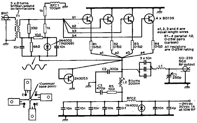
Fig2. LA8AK's experimental 14MHz grounded-collector linear
amplifier using four low-cost BD135 (BD139) npn devices and
providing about 10W rf output.
Last update 2004.12.26
